ASML's high-NA EUV milestone clears the path for next-gen AI chips
After processing 500,000 silicon wafers and hitting 80% operational uptime, ASML says its most advanced chip-making tool is ready for mass production—a development that could reshape how the world's fastest AI processors are manufactured. Intel is first in line; mass-market volumes are expected by 2027-2028. Not every chipmaker is convinced the economics work yet.
What Happened
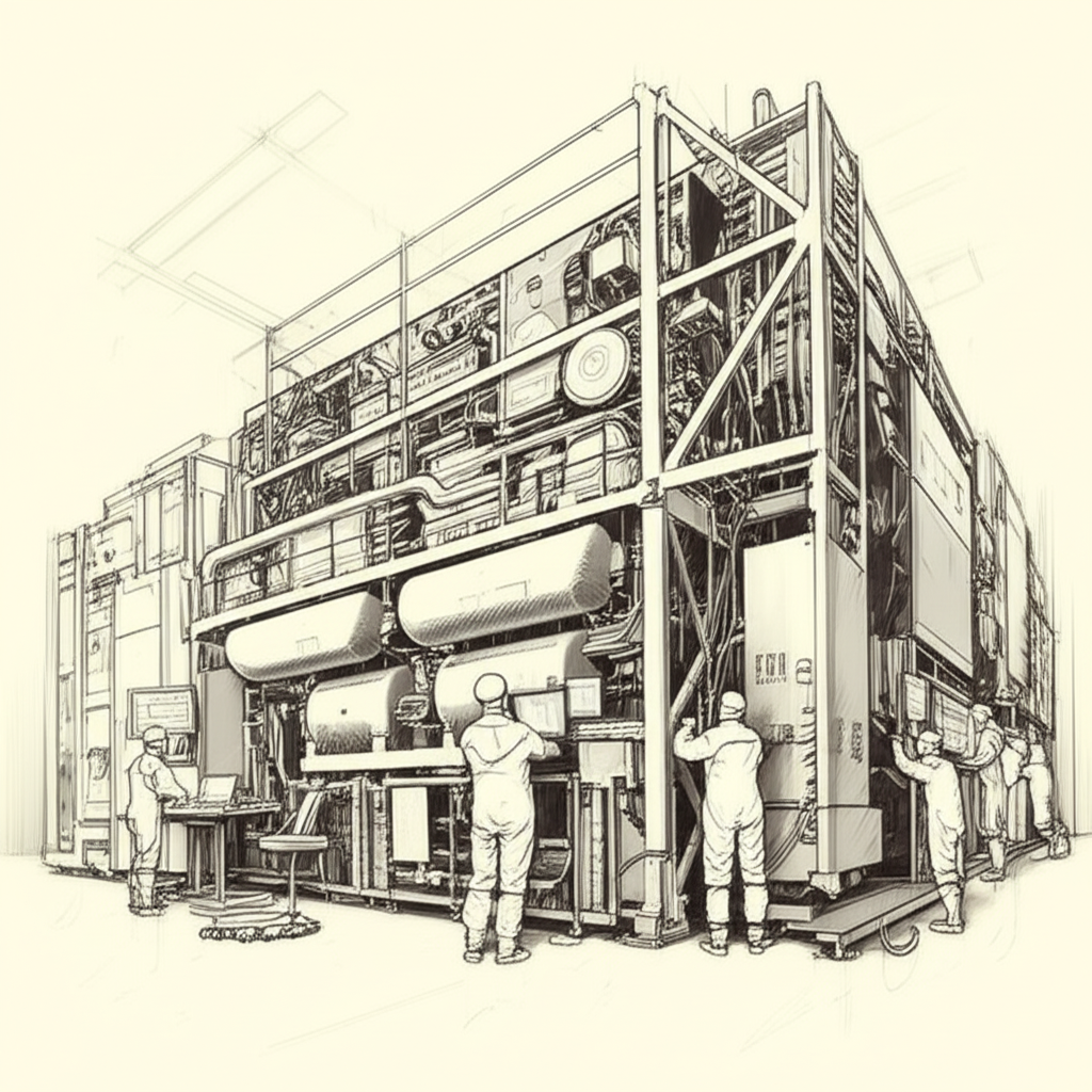
ASML, the Dutch company that makes the machines used to print circuits onto silicon chips, announced on February 27, 2026 that its next-generation lithography tool—called high-NA EUV—has cleared key production readiness milestones. According to ASML's CTO, the Twinscan EXE:5200B tool has now processed 500,000 silicon wafers during its development phase and achieved roughly 80% uptime, with a target of 90% by the end of 2026.
The technical achievement is significant: high-NA EUV (short for high numerical aperture extreme ultraviolet) can print circuit features as small as 8 nanometers—about 1.7 times smaller than what the current generation of EUV tools can achieve. In practical manufacturing terms, it accomplishes in a single pass what previously required 3 to 4 separate patterning steps, according to imec researcher Geert Vandenberghe.
Intel has already installed the first commercial unit of the tool at one of its fabrication facilities, targeting its 14A process node—Intel's planned chip-manufacturing generation for 2027-2028. Samsung and SK hynix also received units in late 2025 and early 2026, per TrendForce reporting.
Each machine carries a price tag of approximately $400 million, roughly double the cost of ASML's current EUV generation.
Why It Matters
To understand why this matters, it helps to think of chip manufacturing as an extraordinarily precise printing process. Transistors—the on/off switches that make computing possible—are printed onto silicon wafers using light. The smaller you can print them, the more you can fit onto a chip, and the more powerful and efficient that chip becomes.

The current generation of tools (using 0.33 numerical aperture optics) is approaching its physical limits at around the 1.5-nanometer mark. High-NA EUV, with its 0.55 numerical aperture, pushes that boundary further by bending light more tightly to create finer patterns. That is the direct path to the smaller transistors that next-generation AI processors—the chips powering large language models and data centers—will require.
The elimination of 3 to 4 manufacturing steps per chip layer is not just a speed improvement. Fewer steps mean lower long-run costs per wafer, less material waste, and reduced manufacturing complexity. Semiconductor Digest, citing imec research, notes the change also enables chip designers to work with more flexible circuit geometries, unlocking design options that were physically impossible at prior nodes.
The competitive picture is uneven. Intel has committed most aggressively, using the tool to anchor its 14A roadmap. Samsung and SK hynix have units in hand. TSMC—the world's largest contract chipmaker—has taken a more cautious stance, opting to skip high-NA for its upcoming 1.4nm node and planning adoption only at a later generation. The $400 million per-unit price and a 2-to-3-year integration timeline before high-volume production are the primary friction points even for well-resourced chipmakers, per Global Banking and Finance reporting.
If chipmakers successfully integrate the technology on schedule, high-NA EUV mass production could begin arriving in consumer and enterprise AI chips in the 2027-2028 window—aligning with the broader industry push for next-generation AI hardware performance.
Sources
- T2
- T2
- T2
- T2
Stay informed. The best AI coverage, delivered weekly.